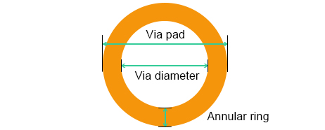
Annular Rings
The copper pad area that remains after a hole is drilled through the pad,
measured from edge of hole to edge of pad.
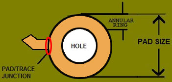
Your inner and outer layer pads should be at least 0.018" larger than the
finish hole size (0.010” for vias). If your design has any pad to trace junction
minimum requirement, add that to the above numbers [0.018" pad + 0.002" junction
should have 0.020" pad]. This will provide a 9mil annular ring for component
pins, 5mil annular ring for vias.
Board material
A printed circuit board (PCB) mechanically supports and electrically connects
electronic components using conductive tracks, pads and other features etched
from copper sheets laminated onto a non-conductive substrate. Components are
generally soldered on the board.
1, classification according to reinforced materials (the most commonly
way)
a. Paper board(FR-1, FR-2, FR-3)
b. Epoxy Glass Cloth (FR-4, FR-5)
c. Composite board (CEM-1, CEM-3)
d. HDI board (RCC-Resin Coated Coppe)
e. Special board (metal board, ceramic board, etc.)
2, classification according to the different types of resin
a. Epoxy resin
b. Polyester resin
c. PI resin (polyimide)
3, classification according to flame retardant properties
a. Flame retardant (UL94-VO, UL94-V1)
b. Non-flame retardant (UL94-HB level)
Board Thickness
The long standing industry standard base PCB thickness is 1/16 inch (0.062").
In addition to the 0.062" thickness the following thicknesses are also available
for Limited Review products: 0.031", 0.047", 0.093", and 0.125". Overall
thickness tolerance is generally within +/- 10% of the given thickness (for 2
and 4 layer boards) and 14% for 6 layer boards.
Blind Via and Buried Via
What is blind via and buried via, and what do they mean for your project? To
understand the answer, first, we need to know what vias are in reference to
printed circuit boards.
What Is a Via?
Vias are the copper-plated holes in the printed circuit board that allows the
layers to connect. The standard via is called a through-hole via, but there are
several disadvantages to using through-hole vias in Surface Mount Technology
(SMT). For this reason, we often use a blind via or buried via instead. A blind
or buried via can be processed in a wide range of different measures, including
plugged copper mask via, a plugged solder mask via, plated via or staggered
via.
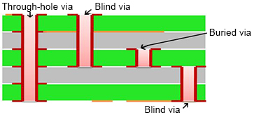
• What Is a Blind Via?
In a blind via, the via connects the external layer to one or more inner
layers of the PCB and is responsible for the interconnection between that top
layer and the inner layers.
• What Is a Buried Via?
In a buried via, only the inner layers of the board are connected by the via.
It is "buried" inside the board and not visible from the outside.
Blind and buried vias are particularly advantageous in HDI PCBs because they
optimize the density of the boards without increasing board size or the number
of board layers you require.
• What Is a Stacked Via and Microvia?
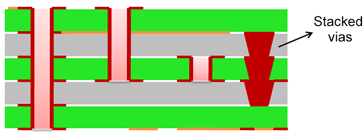
A stacked via is a way to further improve size and density considerations
when manufacturing printed circuit boards — factors that are extremely important
with today's miniaturization and high-signal transmission speed requirements in
many applications.
If you have blind vias with an aspect ratio greater than 1:1, or your
drilling needs cover multiple layers, a stacked via can be the best way to get a
reliable internal connection.
Stacked vias are laminated blind or buried vias, multiple vias inside a
circuit board built together around the same center. Staggered vias are
laminated vias that are not around the same center. The advantages of stacked
vias include not only saving space and increasing density, but greater
flexibility concerning the inner connections, better routing capacity and less
parasitic capacitance. The downside of stacked vias is that they come with a
higher cost than standard through-hole vias or blind/buried vias.
A microvia is merely a very small via. As you can imagine, microvias are very
desirable to PCB designers — the smaller the diameter, the more routing space
you have on the board and the lower the parasitic capacitance, which is
essential for high-speed circuits. However, very small vias also require more
drilling time and more off-center via moves. Microvias as vias with diameters of
less than or equal to 0.1mm.
• Via Type Via Diameter
|
Via
Type
|
Via
Diameter
(max.)
|
Via
Diameter
(min.)
|
Via
Pad
|
Annular
Ring
|
Aspect
Ratio
|
|
Blind via
(mechanical)
|
0.4mm
|
150μm
|
450μm
|
127μm
|
1:1
|
|
Blind via
(laser)
|
0.1mm
|
100μm
|
254μm
|
150μm
|
1:1
|
|
Buried via
(mechanical)
|
0.4mm
|
100μm
|
300μm
|
150μm
|
1:10
|
|
Buried via
(laser)
|
0.4mm
|
100μm
|
225μm
|
150μm
|
1:12
|
Component Side
In order to build your printed circuit board correctly, we must be able to
identify the correct orientation of your design. Component, layer 1, or 'top'
layer should read in facing up. All other layers should line up as though
looking through the board. Please use layer designators, pass through marks, or
correct reading layer text.
Controlled Impedance
The electrical result of manufacturing a circuit board to meet characteristic
impedance specifications. Combination of copper thickness and line width as well
as the dielectric thickness and properties of the base material all contribute
to the impedance value.
Characteristic impedance extends the concept of resistance to AC circuits,
describing not only the relative amplitudes of the voltage and current, but also
the relative phases. When the circuit is driven with direct current (DC) there
is no distinction between impedance and resistance; the latter can be thought of
as impedance with zero phase angle.
Copper (Finished Copper) Weight
This is total thickness of copper on the board surface. The value is
determined from the copper foil thickness, plus plated copper, minus copper
removed during surface preparation. Copper weight is measured in oz /sq foot. 1
oz / sq foot = 0.0012” minimum thickness (height). We offer finished copper
weight of 1-oz., 2-oz., and 3-oz. For multilayer PCBs we offer (1 oz and 2 oz
copper layers).
Drill File (aka. Excellon Drill File)
This is an example of an Excellon drill file format. It will have both X
& Y coordinates along with tool sizes. This will be viewable in any text
editor (notepad). This is the file that governs your finished hole sizes and
locations.
Sample Excellon File format:
M48 INCH
LZ T01C0.015
T02C0.031
T03C0.034
T04C0.037
T05C0.052
T06C0.058
%
T01
X00165Y-03805
X0018Y-03235
X00265Y-00704
X00281Y-01349
X00302Y-03816
![]() Electrical Test
Electrical Test
Electrical continuity (opens) and Isolation (shorts) testing of Circuit
Boards. A net list is created from the customer supplied gerber files and then
electrically compared to the finished pcb. The soldermask layer acts as the mask
to determine what points can be tested. In general, endpoints of all of the nets
are programmed for testing unless they are covered in soldermask, in which case
the closest testable point to the endpoint is tested. The standard testing
parameters used are 100 Volts, Isolation Resistance of 10 M Ohms, Isolation
Distance 0.050”, and Continuity Resistance of 50 Ohms.
Sunstone Circuits uses flying probe (fixtureless) technology to conduct our
electrical testing. We recommend testing all surface mount boards and multilayer
orders.
It's not possible to accurately test boards that have silkscreen on pads. It
is highly recommended that the silkscreen clip option be selected on
electrically tested orders.
ENIG (Electroless Nickel Immersion Gold)
RoHS compliant surface finish, that is also very planar (flat) and durable.
ENIG is recommended for tight pitch, ICs and BGA type of technology. It provides
a good solder joint, allows parts to sit very flat, will withstand multiple
reflow cycles as well as storage of PCBs.
Electroless Deposition - The deposition of conductive material from an
autocatalytic plating solution without the application of electrical
current.
Immersion Plating - The chemical deposition of a thin metallic coating over
certain basis metals that is achieved by a partial displacement of the basis
metal.
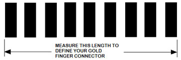
Gold Fingers (Linear Inches)
Edge connectors electroplated with nickel (Ni) and hard gold (Au), good for
wear type applications available for PCBpro and Custom products. (Approx. 200 u”
Ni / Min. 30 u” Au). Utilizing industry standard tie-bar plating protocol to
allow electro plating of Ni and Au after etching and soldermask application.
Price is calculated on the distance (linear inches) between the outside edges of
the outermost connector contacts.
Designer tip: May not be suitable for applications where multiple finger
lengths are required.
With your Au selection, a standard 30-degree bevel will be added to your edge
connector. We can also bevel at 15 or 45 degrees upon request. For multi-layer
boards please insure adequate inner layer back set to allow for the bevel
requested.
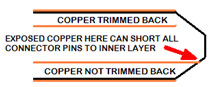
Gold finger connectors typically have the leading edge
beveled in order to ease insertion to the mating connector. When this happens,
inner planes can have exposed copper if they aren’t pulled back from the edge
sufficiently. We will pull your inner layer copper back as shown at the right
above in order to avoid having exposed copper at this location. Exposed copper
can cause a direct short across all terminals of your connector as it is
inserted
HASL (Hot Air Solder Level)
The process of adding solder to the exposed copper features of the circuit
board. The ratio of Tin to Lead in the deposit is approximately 60%/ 40%.
Finished boards are dipped in a molten solder bath and passed through a high
pressure stream of hot air to remove excess solder, resulting in a uniform
solder layer being applied to all exposed copper surfaces. HASL is not an ideal
choice of surface finish for tight pitch or for ICs and BGAs. There will be
variations in solder height from pad to pad and planarity is not a strength of
HASL. Please select Immersion silver or ENIG for these designs. Not a RoHS
compliant finish.
Half-Holes(Castellated Holes)
Plated half holes(castellated holes)are holes that made off the edge of the
boards plated with
copper using a specialized process. It is predominantly used for
board-on-board connections, mostly where two printed circuit boards with
different technologies are combined.
Through connecting the PCBs together directly, the whole system is
considerably thinner than a comparable connection with multi-pin connectors.The
plated edges are also useful in producing mini PCB modules.
Plated half holes are available in both standard PCB and advanced PCB. For
standard PCB service, the minimum diameter of castellated holes is 0.6 mm. If
you need smaller castellated holes please ask our sale to offer advanced PCB
service. And the minimum distance between two Plated half holes is 0.55 mm.
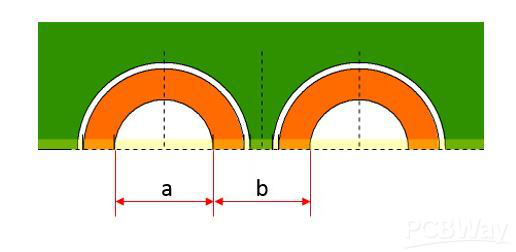
So how to manufacture the Plated half holes? The plating is protected from
mechanical damaging by setting back the copper shell.Therefore the plated
half-holes can be milled precisely and improve the process reliability
strongly
Layer Sequence
We do not require you to map the layers from your files during the order
process to help save you time. In order to be sure we build the layers in the
correct order, provide a readme with the layer order or name the files in a
logical manner. For example:
copper_top.grb
inner1.grb
inner2.grb
copper_bot.grb
silk_top.grb
silk_bot.grb
smask_top.grb
smask_bot.grb
paste_top.grb
paste_bot.grb
ncdrill.txt
drill_dwg.grb
fab_dwg.grb
Layer stack-up
Stack-up refers to the arrangement of copper layers and insulating layers
that make up a PCB prior to board layout design. While a layer stack-up allows
you to get more circuitry on a single board through the various PCB board
layers, the structure of PCB stack-up design confers many other advantages:
. A PCB layer stack can help you minimize your circuit's vulnerability to
external noise as well as minimize radiation and reduce impedance and crosstalk
concerns on high-speed PCB layouts.
. A good layer PCB stack-up can also help you balance your need for low-cost,
efficient manufacturing methods with concerns about signal integrity issues
. The right PCB layer stack can enhance the Electromagnetic Compatibility of
your design as well.
Why need stack-up?
Before designing a multi-layer PCB, designers need to first determine the
circuit board structure based on the size of the circuit, the size of the
circuit board, and the EMC requirements. That is, decide whether to use 4 layers
or 6 layers. More layers of circuit boards. After the number of layers is
determined, the placement of the inner layer and how to distribute different
signals on these layers are determined.
Planning the multilayer PCB stack-up configuration is one of the most
important aspects in achieving the best possible performance of a product. A
poorly designed substrate, with inappropriately selected materials, can degrade
the electrical performance of signal transmission increasing emissions and
crosstalk and can also make the product more susceptible to external noise.
These issues can cause intermittent operation due to timing glitches and
interference dramatically reducing the products performance and long term
reliability. In contrast, a properly built PCB substrate can effectively reduce
electromagnetic emissions, crosstalk and improve the signal integrity providing
a low inductance power distribution network. And, looking from a fabrication
point of view, can also improved manufacturability of the product.
Minimum Traces & Spacing
Trace width and the space between traces are used to define the complexity of
your design. We use this information for pricing and to properly align your
order in our manufacturing products. The smaller or more tightly packed the
features of your board are, the more difficult it will be to manufacture. When
ordering your boards you will need to know the minimum trace size as well as the
minimum copper to copper spacing present in your design.
Non-Plated Holes (NPTH)
A hole in a printed board that does not contain plating or other type of
conductive reinforcement. Generally used for mounting of components to a circuit
board or a circuit board to a larger portion of a project.
We recommend that you include a drill drawing to identify the non-plated
holes in your design.
Non-Plated holes should maintain a minimum clearance of 0.010” from any
conductive surface.
Plated Through Holes (PTH)
A hole with plating on its walls that makes an electrical connection between
conductive patterns on internal layers, external layers, or both, of a printed
board.
All drill sizes will be treated as PTH unless NPTH is specified in the
Drawing, Print, Drill file, drill tool description text file, or identified with
a special note, for example “ 0.125 holes to be non plated” In addition,
landless holes identified in the Gerber files will be treated as non plated:
holes without pads, holes designated with a crosshair target, or holes with a
significantly smaller pad (i.e. 0.125" holes with 0.050" unsupported pads).
All holes in the drill file regardless of definition will be treated as
plated holes. This means that they will have the hole size increased to
accommodate plating, will be drilled at primary drill, and may or may not be
plated (depending on presence of pads, proximity to copper features, or size of
the drilled hole).
If drawing or tool description is different than the size specified within
the drill file, we will use the drill file to determine finished hole size (For
“Full Review” (NRE) these errors are reported for customer clarification before
manufacturing can begin).
All orders placed as “1 layer” will be treated as single sided and the holes
barrels will be non-plated.
Surface finish
There are many kinds of surface treatments, and mainly shown with 5 types,
they are HASL, OSP, ENIG, Immersion tin and Immersion silver.
HASL or HASL LF:
HASL should be the most widely used surface treatment technology. When the
hot air is leveled, the solder and copper form a copper tin metal compound at
the junction, and the thickness thereof is approximately 1 to 2 mils. HASL
provides a very reliable solder joint and shelf life. HASL makes component
soldering very effective, but due to the thickness of HASL coating, the
planarity of the surface may be unsuitable for fine-pitch components. The HASL
deposit is made from a eutectic blend of tin and lead.
ENIG (Immersion gold):
ENIG is just one process that covers one thick layer of nickel-gold alloy
with good electrical properties over copper, which processes long-term
protection for PCBs to reach excellent mechanical properties. What’s more, ENIG
surface holds the special tolerance with the environment that other finishes
fail to meet. Its capability to prevent the copper dissolution also brings a
good performance to lead free soldering.
OSP:OSP surface (Organic solder ability preservative) is a process to
generate a layer of organic film over clear bare copper in chemical way. This
layer of organic film is resistant to oxidation, thermal shock and wetting ,
which protect the copper surface from rust under normal environment. Meanwhile,
it could also be easily removed in the subsequent high temperature welding for
better soldering. Its simple process and low cost brings its wide usage in PCB
production.
Immersion silver: The immersion silver process is relatively simple and fast.
There is no need to apply a thick layer of armor to the PCB board, but also
provides good electrical and solder ability for the PCB board in a hot, wet and
polluted environment. The disadvantage is that it will lose its luster. And it
also has good storage property.
Immersion Tin: Immersion Tin surface is adopted for its good flatness and
lead free nature. However, Cu/Sn intermetallic compounds with poor solder
ability are easily generated in the process. The biggest weakness of immersion
tin surface is its short life, especially when stored in high temperature and
high humidity environment, Cu/Sn intermetallic compounds will increase until the
loss of solder ability.
· Comparison of cost and solderability
Cost: Electroplating nickel gold > ENIG > Immersion silver>
Immersion tin > HASL > OSP.
Actual solderability: Electroplating nickel gold> HASL > OSP > ENIG
>Immersion silver >Immersion tin
PCB surface finish is a coating between a component and a bare board PCB. It
is applied for two basic reasons: to ensure solderability, and to protect
exposed copper circuitry. As there are many types of surface finishes,selecting
the right one is no easy task, especially as surface mounts have become more
complex and regulations such as RoHS and WEEE have changed industry
standards.
HASL(Hot Air Solder Leveling) / Lead Free HASL
HASL is the predominant surface finish used in the industry. The process
consists of immersing circuit boards in a molten pot of a tin/lead alloy and
then removing the excess solder by using 'air knives', which blow hot air across
the surface of the board.
Pros: Low-cost, Available, Repairable
Cons: Uneven Surfaces, Not good for fine pitch components, Thermal Shock, Not
good for plated through-hole (PTH), Poor wetting
OSP (Organic Solderability Preservative)
OSP is a water-based, organic surface finish that is typically used for
copper pads. It selectively bonds to copper and protects the copper pad before
soldering. OSP is environmentally friendly, provides a coplanar surface, is
lead-free, and requires low equipment maintenance. However, it’s not as robust
as HASL and can be sensitive while handling.
Pros:Lead-free, Flat surface, Simple process, Repairable
Cons:Not good for PTH, Sensitive, Short Shelf life
ENIG (Electroless Nickel Immersion Gold )
ENIG is quickly becoming the most popular surface finish in the industry.
It’s a double layer metallic coating, with nickel acting as both a barrier to
the copper and a surface to which components are soldered. A layer of gold
protects the nickel during storage. ENIG is an answer to major industry trends
such as lead-free requirements and rise of complex surface components
(especially BGAs and flip chips), which require flat surfaces. But ENIG can be
expensive, and at times can result in what is commonly known as “black pad
syndrome,” a buildup of phosphorous between the gold and nickel layers that can
result in fractured surfaces and faulty connections.
Pros: Flat surfaces, Strong, Lead-free, Good for PTH
Cons: Black pad syndrome, Expensive, Not good for rework
Stencil
The sole purpose of a stencil is to transfer solder paste to a bare circuit
board. A stainless foil is laser cut creating an opening for every surface mount
device on the board. Once the stencil is properly aligned on top of the board,
solder paste is applied over the openings (making a single pass, using a metal
squeegee blade). When the foil is separated from the board, bricks of solder
paste remain, ready for placement of the SMD. This process, as opposed to hand
soldering methods, ensures consistency and saves time.
Foil thickness and aperture opening size control the volume of paste
deposited on the board. Too much solder paste causes solder balling, bridging,
and tomb-stoning. A lack of solder paste creates insufficient solder joints. All
of which compromise the electrical functionality of the board.
Proper foil thickness is chosen based on the types of devices being loaded on
the board. Component packages such as 0603 capacitors or 0.020” pitch SOIC’s,
will require a thinner stencil than larger packages such as 1206 capacitors or
0.050” pitch SOIC’s. Stencil thickness ranges from 0.001” to 0.030”. The typical
foil thickness used on the majority of boards is anywhere from 0.004” to
0.007”.
Via Covering
Vias not covered
It means that the vias are exposed and the surface finish is applied to via
barrel.
The solder paste might get into the vias and cause poor or non-existent
solder joints.
Tenting vias
It means that the vias are simply covering by soldermask ink.No additional
process steps is required during fabrication.
Covering the annular ring and vias with soldermask ink in order to prevent
exposure to the elements and reduce accidental shorting or contact with the
circuit.
Plugged Vias with non conductive media (eg. Epoxy/resin, solder mask ink)
The conductive vias in BGA requires plugged vias. Because solder paste might
wick away from the intended pad and flow down into the via, then creating poor
or non-existent solder joints during assembly.
The diameter of the plugged vias requires to be smaller than 0.5mm.